| 如果你不能正常浏览页面,请点击此处。 |
 |
| |
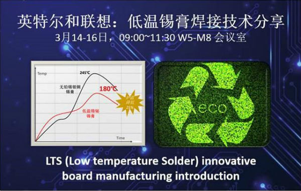
| 低温焊膏应用技术是SMT领域一项重要的技术壁垒。低温焊膏具有温度需求低,金属成本低,能耗小,绿色环保等优势。为了突破技术难关, Intel和联想在2015年初就开始推进这个项目,历经将近2年的时间,完成了多项技术创新以及流程优化,目前使用了最新型低温锡膏的电脑产品已经通过了60余项权威的可靠性测试,小批量的试产也取得了非常好的成绩,达到了进入全面量产的条件。从环保方面来看,相对于现在使用的锡银铜(SAC)金属成分锡膏,低温锡膏焊接的峰值温度由250~260°C降至180~190°C,由此带来的好处是极大地降低工厂的能源消耗(比如电能)和温室气体(比如二氧化碳)排放。 |
| |
| Theme: Intel-Lenovo LTS (Low temperature Solder) innovative board manufacturing introduction and sharing |
| 3/14-3/16 09:00~11:30 am on meeting room @ W5-M8 |
| Agenda: |
- Introduction & Motivation
- Breakthrough Technology
- Cost Savings
- Energy & Environment
- Faster Technology Scaling
- Next big plan
|
| |
| 英特尔和联想:低温锡膏焊接技术分享 |
| 3月14-16日,每天上午09:00~11:30 W5-M8 会议室 |
| 议题: |
- 低温锡膏焊接的介绍及效益
- 技术突破
- 成本节约
- 节能与环保
- 更快的技术扩展
- 未来展望
|
| |
| 观众免费,座位有限,报名从速! |
| |
| Intel Contact: |
| Shirley Zhang |
| Email: [email protected] |
| Phone: +86-21- 2207 1274 |
| |
感谢接收此邮件。如您想退订请点击此处。
Click here to unsubscribe from this list only.
To unsubscribe from all SEMI email promotions, please email us at [email protected].
Copyright® 2017 SEMI. All rights reserved.
SEMI is headquartered at 673 South Milpitas Blvd. Milpitas, CA 95035, Tel: 1.408.943.6900, Fax: 1.408.428.9600, Web site: www.semi.org |