

| 主办方: |  |
| 承办方: |  |
| 独家钻石赞助: |  |
| 09:00-09:30 | 论坛注册 Registration |
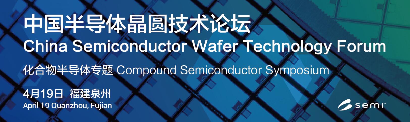
| 09:30-09:40 | 欢迎致辞 Welcome Remark 吕刚 福建省泉州市人民政府副市长 |
| 09:40-10:10 | 主旨演讲 Keynote Speech RF-SOI: 助推5G移动互联 RF-SOI: Enabling 5G Connectivity 王庆宇 Jeffrey Wang 上海新傲科技股份有限公司总经理 CEO of Shanghai Simgui Technology Co., Ltd |
| 10:10-10:40 | 坩埚下降法蓝宝石晶体生长技术及其在LED中的应用 Sapphire growth by vertical gradient freeze method and its applications in LEDs 王江波博士 Dr. Jiangbo Wang 华灿光电副总裁 VP of HC SEMITEK |
| 10:40-11:10 | 碳化硅大尺寸晶圆及外延材料技术进展 SiC Substrate and Its Epitaxial Materials Technology 冯淦博士 Dr. Gan Feng 瀚天天成电子科技(厦门)有限公司总经理 General Manager of Epiworld International Co., LTD |
| 11:10-11:40 | 化合物半导体-我国半导体产业的突破口 Compound Semiconductor-the Breakthough of Semiconductor Industry in China 朱邵歆博士 Dr. Shaoxin Zhu 中国电子信息产业发展研究院(赛迪研究院)集成电路研究所高级工程师 Senior Engineer of China Center for Information Industry Development IC Industry Research Institute |
| 11:40-13:30 | 午餐 |
| 13:30-14:00 | 氮化镓衬底晶片的研究和产业化进展 Research and Industrial Development on GaN Substrate Wafer 徐科博士 Dr. Ke Xu 苏州纳维科技有限公司董事长 Chairman of Nanowin |
| 14:00-14:30 | 碳化硅单晶衬底产业化进展 SiC Single Crystal Substrate Industrial Development 彭同华博士 Dr. Tonghua Peng 天科合达副总经理 Vice General Manager of TankeBlue Semiconductor |
| 14:30-15:00 | 大尺寸碳化硅晶圆材料制造技术进展 Large Scale SiC Wafer Material Manufacturing Technology 张洁 Jack Zhang 福建北电新材料科技有限公司副总经理 Vice General Manager of Norstel |
| 15:00-15:30 | 蓝宝石图形衬底形貌与缺陷检测方法 Introduction to the Inspection Methods of Pattern Shape and Defects of Patterned Sapphire substrate (PSS) 谢斌晖博士 Dr. Pinhui Hsieh 福建晶安光电有限公司总经理助理 Assistant General Manager of JINAN OPTOELECTRONICS |
| 15:30-16:00 | 砷化镓及磷化铟晶圆技术介绍 GaAs and InP Substrate Wafer Technology 任殿胜博士 Dr. Diansheng Ren 北京通美晶体技术有限公司总监 Director of AXT, Inc. |
| 16:00-16:30 | 宽禁带半导体材料的晶体生长技术 Crystal Growth of Wideband Gap Semiconducting Materials Dr.P.S.Raghavan Chief Technology Officer of GT Advanced Technology |
| 17:30-20:00 | 产业招待晚宴 Industry Reception Dinner |
| 戚发鑫 / Daniel Qi | 黄晓依 / Sophia Huang |
| Tel: 021-6027.8576 | Tel: 021.6027.8553 |
| Email: [email protected] | Email: [email protected] |
感谢接收此邮件。如您想退订请点击此处。
Click here to unsubscribe from this list only.
To unsubscribe from all SEMI email promotions, please email us at [email protected].
Copyright® 2018 SEMI. All rights reserved.
SEMI China is at 8th floor, 2nd Building, No. 1158, Zhang Dong Road, Shanghai, China, 201203
Tel: +86.21.6027.8500, Fax: +86.21.6027.8511, Web site: www.semichina.org